
Hartley Oscillator
Hartley Oscillator
Broad Goal of the experiment: To analyze output waveform of Hartley Oscillator. To verify theoretical and practical value of frequency of oscillation of Hartley Oscillator. To design Hartley Oscillator and verify the de...
Aim
Broad Goal of the experiment:
- To analyze output waveform of Hartley Oscillator.
- To verify theoretical and practical value of frequency of oscillation of Hartley Oscillator.
- To design Hartley Oscillator and verify the design.
Theory
An amplifier circuit simply increases the signal strength. But while amplifying, it just increases the strength of its input signal whether it contains information or some noise along with information. This noise or some disturbance is introduced in the amplifiers because of their strong tendency to introduce hum due to sudden temperature changes or stray electric and magnetic fields. Therefore, every high gain amplifier tends to give noise along with signal in its output, which is very undesirable.
The noise level in the amplifier circuits can be considerably reduced by using negative feedback done by injecting a fraction of output in phase opposition to the input signal.
What is a Feedback Amplifier?
The feedback-amplifier can be defined as an amplifier which has feedback lane that exists between o/p to input. In this type of amplifier, feedback is the limitation which calculates the sum of feedback given in the following amplifier. The feedback factor is the ratio of the feedback signal and the input signal.
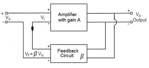
Types of Feedback Amplifiers:
1. Positive Feedback Amplifier:
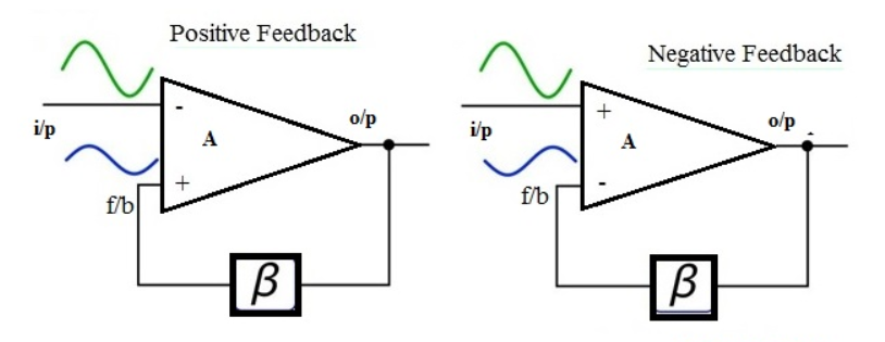
The positive feedback can be defined as when the feedback current otherwise voltage is applied for increasing the i/p voltage, then it is named as positive feedback. Direct feedback is another name of this positive feedback. Because positive feedback generates unnecessary distortion; it is not often used in amplifiers. But, it amplifies the original signal power and can be used in oscillator circuits.
2. Negative Feedback Amplifier:
The negative feedback can be defined as if the feedback current otherwise voltage can be applied for reducing the amplifier i/p, then it is called as negative feedback. Inverse feedback is another name of this negative feedback. This kind of feedback is regularly used in amplifier circuits.
What is an Oscillator?
An Oscillator is basically an Amplifier with “Positive Feedback”, or regenerative feedback (in-phase) and without any external input signal that generates an output waveform of a desired frequency.
An oscillator is basically a waveform generator which generates an output waveform, which oscillates with constant amplitude & constant desired frequency.
Barkhausen criterion:
The frequency of oscillation at which sinusoidal oscillator operates is the frequency for which the total shift introduced, as the signal proceeds from the input terminals, through the amplifier and feedback network, and back again to the input, is precisely zero (or an integral multiple of 2*Π).
(OR)
Stated simply the condition A*β = -1 at ω= ωo, i.e. the magnitude of loop gain should be one and phase of loop gain should be unity (the feedback network introduces 1800 phase shift, the other 1800 phase shift is provided by Amplifier) is called Barkhausen criterion.
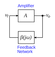
A closed loop system with negative feedback can be represented by a transfer function = A/(1+A*β). Often feedback network consists of only resistive elements and is independent of frequency but amplifier gain is a function of frequency. Hence the loop gain A*β is a function of frequency. There may exist a frequency ωo at which its magnitude is one and phase is 1800 i.e. A*β = -1 (Barkhausen criterion).
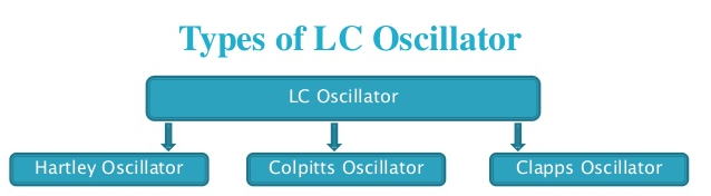
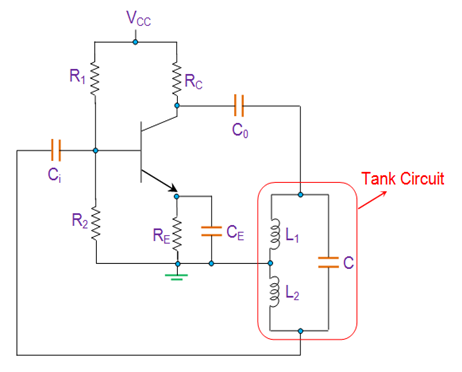
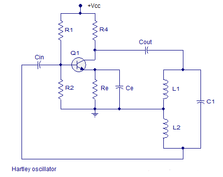
In the Hartley Oscillator the tuned LC circuit is connected between the collector and the base of a transistor amplifier. As far as the oscillatory voltage is concerned, the emitter is connected to a tapping point on the tuned circuit coil.
The feedback part of the tuned LC tank circuit is taken from the centre tap of the inductor coil or even two separate coils in series which are in parallel with a variable capacitor, C as shown.
An Hartley Oscillator circuit can be made from any configuration that uses either a single tapped coil (similar to an autotransformer) or a pair of series connected coils in parallel with a single capacitor as shown below.
Basic Hartley Oscillator Design:
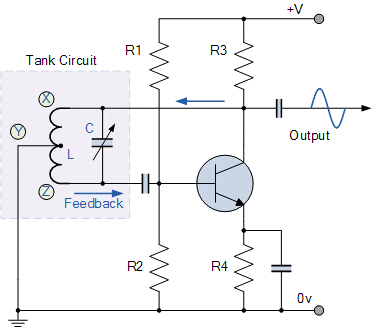
When the circuit is oscillating, the voltage at point X (collector), relative to point Y(emitter), is 1800 out-of-phase with the voltage at point Z (base) relative to point Y. At the frequency of oscillation, the impedance of the Collector load is resistive and an increase in Base voltage causes a decrease in the Collector voltage.
Then there is a 1800 phase change in the voltage between the Base and Collector and this along with the original 1800 phase shift in the feedback loop provides the correct phase relationship of positive feedback for oscillations to be maintained.
The amount of feedback depends upon the position of the “tapping point” of the inductor. If this is moved nearer to the collector the amount of feedback is increased, but the output taken between the Collector and earth is reduced and vice versa. Resistors, R1 and R2 provide the usual stabilizing DC bias for the transistor in the normal manner while the capacitors act as DC-blocking capacitors.
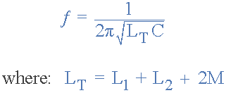
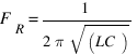
In this Hartley Oscillator circuit, the DC Collector current flows through part of the coil and for this reason the circuit is said to be “Series-fed” with the frequency of oscillation of the Hartley Oscillator being given as.
Note:
LT is the total cumulatively coupled inductance if two separate coils are used including their mutual inductance, M.
The frequency of oscillations can be adjusted by varying the “tuning” capacitor, C or by varying the position of the iron-dust core inside the coil (inductive tuning) giving an output over a wide range of frequencies making it very easy to tune. Also the Hartley Oscillator produces an output amplitude which is constant over the entire frequency range.
Procedure
- There are two parts in this experiment.
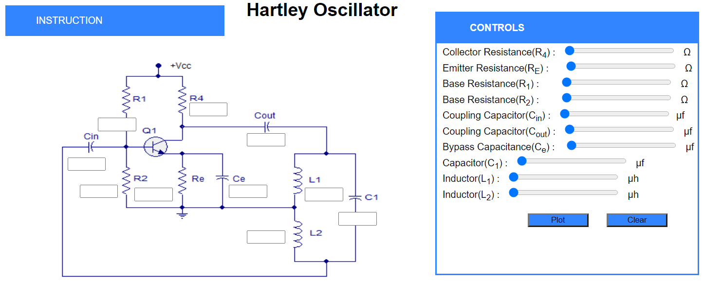
- In Part 1, the initial values of the circuit are given in the introducton dropdown, students just have to set the values using the controls section.
- Also,Students can use left and right arrow keys to set a particular component value.
- After setting the values, there are two buttons available plot and clear.
- Plot will check whether all the values entered are correct and Output will be shown in the Output section.
- Clear will clear the contents of input boxes and the output graph.
- Students can check their calculated output with the simulator output in the check output section.
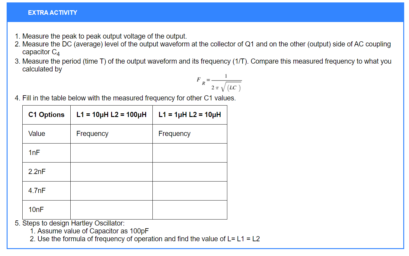
- Part 2 contains extra activity where you have to solve questions as directed and perform the experiment for given values of Capcitors and Inductors.
Procedure for Pre-Test:
- To start the test click on start button.
- After Answering the questions, click on submit to submit the test.
- After submitting the Test,you need to download your submitted answers using download button first only then you can see the answers otherwise you will not be able to download your submitted answers
Pre-Test
click on start to start the quiz
Simulation
INSTRUCTION
- Part 1:Use these values and perform the experiment.
- Set R1=100kΩ
- Set R2=5kΩ
- Set R4=1kΩ
- Set Re=10kΩ
- Set C1=0.01μF
- Set L1=10mH
- Set L2=20mH
- Set Cin=100nF
- Set Cout=0.1μF
- Set Ce=100nF
- Note: The values of Capacitors and Inductors should STRICTLY lie in range Of micro units as shown in Controls Section.
- Part 2:Solve questions as directed and perform the experiment for given values of Capcitors and Inductors.
CONTROLS
Emitter Resistance(RE) : Ω
Base Resistance(R1) : Ω
Base Resistance(R2) : Ω
Coupling Capacitor(Cin) : μF
Coupling Capacitor(Cout) : μF
Bypass Capacitance(Ce) : μF
Capacitor(C1) : μF
Inductor(L1) : μh
Inductor(L2) : μh
OUTPUT GRAPH
Check Output
- What is the Output Frequency of The Graph Shown?
( Note: Your answer should be rounded up to 3 decimals)
EXTRA ACTIVITY
- Measure the peak to peak output voltage of the output.
- Measure the DC (average) level of the output waveform at the collector of Q1 and on the other (output) side of AC coupling capacitor C4
- Measure the period (time T) of the output waveform and its frequency (1/T). Compare this measured frequency to what you calculated by
- Fill in the table below with the measured frequency for other C1 values.
- Steps to design Hartley Oscillator:
- Assume value of Capacitor as 100pF
- Use the formula of frequency of operation and find the value of L= L1 = L2
| C1 Options | L1 = 10μH L2 = 100μH | L1 = 1μH L2 = 10μH |
|---|---|---|
| Value | Frequency | Frequency |
| 1nF | ||
| 2.2nF | ||
| 4.7nF | ||
| 10nF |
Post-Test
Task 1:
Observe the changes in the output waveform by changing values of resistors in the circuit diagram and keeping values of components in tank circuit as constant.
Task 2:
Design tank circuit for Hartley Oscillator for frequency of oscillation f = 3MHz and frequency of oscillation f = 5MHz
After the design, verify your design by putting designed values of tank circuit in simulator and cross verify the frequency of oscillation.
References
Books Referred:
- Electronic Devices and Circuit Theory by Robert Boylestad and Louis Nashelsky, 11th Edition.
- Electronic Circuits Analysis and Design by Donald A. Neaman, 3rd Edition.
Websites:
Generate PDF
Please read the following instructions carefully!
- Take the snapshot of your observations and Graphs.
- Save them on your PC as .png files.
- Click on the button to redirect to the doc file.
- Download it as Microsoft Word(.docx) file.
- Post your results and graphs in the space provided in the doc file.
- Write your Conclusion.
- Save it as .pdf file.
- Your Experiment write-up is ready.
